- 您现在的位置:买卖IC网 > Sheet目录2009 > MAX3676EHJ+T (Maxim Integrated Products)IC CLOCK RECOVERY 32-TQFP
MAX3676
622Mbps, 3.3V Clock-Recovery and
Data-Retiming IC with Limiting Amplifier
12
______________________________________________________________________________________
Optical receivers, incorporating transimpedance
preamplifiers and limiting postamplifiers, can signifi-
cantly clean up the effects of dispersion and attenua-
tion. In addition, these amplifiers can provide fast
transitions with minimal aberrations to the subsequent
CDR blocks. However, these stages also add distor-
tions to the midpoint crossing, contributing to timing jit-
ter. Timing jitter is one of the most critical technical
issues to consider when developing optical receivers
and CDR circuits.
A better understanding of the different sources of jitter
helps in the design and application of optical receiver
modules and integrated CDR solutions. SDH/SONET
specifications are well defined regarding the amount of
jitter tolerance allowed at the inputs of optical receivers,
as well as jitter peaking requirements, but they do little
to define the different sources of jitter. The jitter that
must be tolerated at an optical receiver input involves
three significant sources, all of which are present in
varying degrees in typical receiver systems:
1) Random jitter (RJ)
2) Pattern-dependent jitter (PDJ)
3) Pulse-width distortion (PWD)
Random Jitter
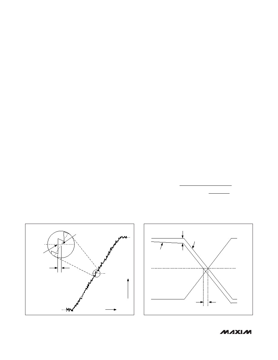
RJ is caused by random noise present during edge
transitions (Figure 8). This random noise results in ran-
dom midpoint crossings. All electrical systems gener-
ate some random noise; however, the faster the speed
of the transitions, the lower the effect of noise on ran-
dom jitter. The following equation is a simple worst-
case estimation of random jitter:
RJ (rms) = (rms noise)/(slew rate)
Pattern-Dependent Jitter
PDJ results from wide variations in the number of con-
secutive bits contained in NRZ data streams working
against the bandwidth requirements of the receiver
(Figure 9). The location of the lower -3dB cutoff fre-
quency is important, and must be set to pass the low
frequencies associated with long consecutive bit
streams. AC-coupling is common in optical receiver
design.
When using a preamplifier with a highpass frequency
response, select the input AC-coupling capacitor, CIN,
to provide a low-frequency cutoff (fC) one decade lower
than the preamplifier low-frequency cutoff. As a result,
the PDJ is dominated by the low-frequency cutoff of
the preamplifier.
When using a preamplifier without a highpass response
with the MAX3676, the following equation provides a
good starting point for choosing CIN:
where tL = duration of the longest run of consecutive
bits of the same value (seconds); PDJ = maximum
C
-t
1.25k
In
PDJ BW
IN
L
≥
() ()( )
Ω
.
1
05
MIDPOINT
RANDOM
JITTER
ACTUAL
MIDPOINT
CROSSING
DESIRED
MIDPOINT
CROSSING
0–1
TRANSITION
WITH RANDOM
NOISE
TIME
AMPLITUDE
Figure 8. Random Jitter on Edge Transition
AMPLITUDE
TIME
MIDPOINT
LONG
CONSECUTIVE
BIT STREAM
0-1-0 BIT STREAM
LF DROOP
LF PDJ
Figure 9. Pattern-Dependent Jitter Due to Low-Frequency
Cutoff
发布紧急采购,3分钟左右您将得到回复。
相关PDF资料
MAX3872ETJ+T
IC DATA RECOVERY W/AMP 32-TQFN
MAX3873AETP+T
IC RECOV/RETIME 2.5GBPS 20TQFN
MAX3886ETN+T
IC MULTIRATE CDR SER/DES56-TQFN
MAX3991UTG+T
IC DATA RECOVERY W/AMP 24-TQFN
MAX3992UTG+T
IC DATA RECOVERY W/EQ 24-TQFN
MAX504EPD+
IC DAC 10BIT 5V LP SER 14-DIP
MAX507AENG+
IC DAC 12BIT W/REF 24-DIP
MAX5100AEUP+T
IC DAC 8BIT QUAD R-R 20TSSOP
相关代理商/技术参数
MAX3676EHJ-T
功能描述:时钟发生器及支持产品 622Mbps 3.3V Clock Recovery RoHS:否 制造商:Silicon Labs 类型:Clock Generators 最大输入频率:14.318 MHz 最大输出频率:166 MHz 输出端数量:16 占空比 - 最大:55 % 工作电源电压:3.3 V 工作电源电流:1 mA 最大工作温度:+ 85 C 安装风格:SMD/SMT 封装 / 箱体:QFN-56
MAX3677CTJ+
制造商:Microsemi Corporation 功能描述:+3.3V, LOW-JITTER CLOCK GEN W/MULT OUT - Trays 制造商:Microsemi Corporation 功能描述:Microsemi MAX3677CTJ+ Clocks - Timers 制造商:MICROSEMI CONSUMER MEDICAL PRODUCT GROUP 功能描述:IC CLOCK GENERATOR PROGR 32TQFN 制造商:Microsemi Corporation 功能描述:IC CLOCK GENERATOR PROGR 32TQFN
MAX3677CTJ+T
制造商:Microsemi Corporation 功能描述:+3.3V, LOW-JITTER CLOCK GEN W/MULT OUT - Tape and Reel
MAX3677EVKIT+
制造商:Microsemi Corporation 功能描述:MAX3677 EVALUATION KIT - Boxed Product (Development Kits) 制造商:MICROSEMI CONSUMER MEDICAL PRODUCT GROUP 功能描述:KIT EVALUATION MAX MAX3677
MAX3678EVKIT+
功能描述:时钟和定时器开发工具 Not Available From Mouser RoHS:否 制造商:Texas Instruments 产品:Evaluation Modules 类型:Clock Conditioners 工具用于评估:LMK04100B 频率:122.8 MHz 工作电源电压:3.3 V
MAX3678UTN+
功能描述:时钟发生器及支持产品 Low-Jitter Frequency Synthesizer RoHS:否 制造商:Silicon Labs 类型:Clock Generators 最大输入频率:14.318 MHz 最大输出频率:166 MHz 输出端数量:16 占空比 - 最大:55 % 工作电源电压:3.3 V 工作电源电流:1 mA 最大工作温度:+ 85 C 安装风格:SMD/SMT 封装 / 箱体:QFN-56
MAX3678UTN+T
功能描述:时钟发生器及支持产品 Low-Jitter Frequency Synthesizer RoHS:否 制造商:Silicon Labs 类型:Clock Generators 最大输入频率:14.318 MHz 最大输出频率:166 MHz 输出端数量:16 占空比 - 最大:55 % 工作电源电压:3.3 V 工作电源电流:1 mA 最大工作温度:+ 85 C 安装风格:SMD/SMT 封装 / 箱体:QFN-56
MAX3679AETJ+
功能描述:时钟发生器及支持产品 3.3V Low-Jitter Crystal to LVPECL RoHS:否 制造商:Silicon Labs 类型:Clock Generators 最大输入频率:14.318 MHz 最大输出频率:166 MHz 输出端数量:16 占空比 - 最大:55 % 工作电源电压:3.3 V 工作电源电流:1 mA 最大工作温度:+ 85 C 安装风格:SMD/SMT 封装 / 箱体:QFN-56